New Method for Making Green LEDs Enhances Efficiency, Brightness
Researchers at the University of Illinois at Urbana Champaign have developed a new method for making brighter and more efficient green light-emitting diodes (LEDs). Using an industry-standard semiconductor growth technique, they have created gallium nitride (GaN) cubic crystals grown on a silicon substrate that are capable of producing powerful green light for advanced solid-state lighting.
"This work is very revolutionary as it paves the way for novel green wavelength emitters that can target advanced solid-state lighting on a scalable CMOS-silicon platform by exploiting the new material, cubic gallium nitride," said Can Bayram, an assistant professor of electrical and computer engineering at Illinois who first began investigating this material while at IBM T.J. Watson Research Center several years ago.
"The union of solid-state lighting with sensing (e.g. detection) and networking (e.g. communication) to enable smart (i.e. responsive and adaptive) visible lighting, is further poised to revolutionize how we utilize light. And CMOS-compatible LEDs can facilitate fast, efficient, low-power, and multi-functional technology solutions with less of a footprint and at an ever more affordable device price point for these applications."
Typically, GaN forms in one of two crystal structures: hexagonal or cubic. Hexagonal GaN is thermodynamically stable and is by far the more conventional form of the semiconductor. However, hexagonal GaN is prone to a phenomenon known as polarization, where an internal electric field separates the negatively charged electrons and positively charged holes, preventing them from combining, which, in turn, diminishes the light output efficiency.
Until now, the only way researchers were able to make cubic GaN was to use molecular beam epitaxy, a very expensive and slow crystal growth method when compared to the widely used metal-organic chemical vapor deposition (MOCVD) method that Bayram used.
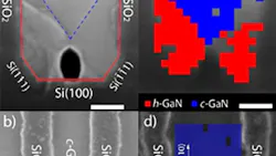
Bayram and his graduate student Richard Liu made the cubic GaN by using lithography and isotropic etching to create a U-shaped groove on Si (100). This non-conducting layer essentially served as a boundary that shapes the hexagonal material into cubic form.
"Our cubic GaN does not have an internal electric field that separates the charge carriers—the holes and electrons," explained Liu. "So, they can overlap and when that happens, the electrons and holes combine faster to produce light."
Ultimately, Bayram and Liu believe their cubic GaN method may lead to LEDs free from the "droop" phenomenon that has plagued the LED industry for years. For green, blue, or ultra-violet LEDs, their light-emission efficiency declines as more current is injected, which is characterized as "droop."
"Our work suggests polarization plays an important role in the droop, pushing the electrons and holes away from each other, particularly under low-injection current densities," said Liu, who was the first author of the paper, ""Maximizing Cubic Phase Gallium Nitride Surface Coverage on Nano-patterned Silicon (100)", appearing Applied Physics Letters.
Having better performing green LEDs will open up new avenues for LEDs in general solid-state lighting. For example, these LEDs will provide energy savings by generating white light through a color mixing approach. Other advanced applications include ultra-parallel LED connectivity through phosphor-free green LEDs, underwater communications, and biotechnology such as optogenetics and migraine treatment.
Enhanced green LEDs aren't the only application for Bayram's cubic GaN, which could someday replace silicon to make power electronic devices found in laptop power adapters and electronic substations, and it could replace mercury lamps to make ultra-violet LEDs that disinfect water.
Analysis: Significance of Lighting Efficiency Improvements
This recent announcement about a significant R&D breakthrough in LED lighting on the Phys Org website is a good occasion for us to take a quick look at where we stand when it comes to lighting: What would the value be in terms of energy and demand reduction and economic savings, if and when new commercialization is achieved for LED breakthroughs such as Urbana’s new Gallium Nitride technology?
The good news when it comes to the current overall U.S. market penetration of more efficient lighting, is that flashlights, exit signs, and traffic signals are all now “mainstream” and are doing very well! But on the “bad news” side, or at least the “room for lots of improvement” side, when we look at the areas where the most energy is being consumed for lighting, the penetration is still mostly in the single-digit percentages, as shown on the chart below:
Source: Adoption of Light-Emitting Diodes in Common Lighting Applications, July 2015, U.S. Department of Energy, page 9.
The reason the breakthrough with GaN could be encouraging is not just due to the technology’s improvements in earlier LED lighting solution efficiency, but also, as indicated in an earlier Phys Org announcement about this technology, the expected 100,000 hour, or 60 year life, for these GaN-based lights.
The U.S. Energy Information Administration’s recent estimate is that lighting consumed 404 billion kWh of electricity in 2015, which they equated with 15% of total electricity consumed in the Commercial and Residential sectors, as well as sizing lighting overall as making up 10% of total U.S. electricity consumption. With the average residential electric bill nationwide coming in at $114 per month (EIA Form 861 at this link), a lot of the lighting-related ten percent per month, or $11.40, is still being wasted as heat in most of our homes (unless you live in an igloo-type dwelling and benefit from the heat off of the bulbs that still convert the majority of their electricity to heat.

